PCB board manufacturing process explained from design files to final inspection
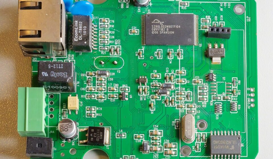
What the PCB board manufacturing process does
The PCB board manufacturing process converts verified design data into a bare printed circuit board that is ready for component assembly. In a typical rigid board build, fabrication starts with manufacturing files and laminate selection. It then moves through imaging, etching, lamination, drilling, copper deposition, plating, solder mask, surface finish, routing, electrical testing, and final inspection.
The flow is not identical for every board. A simple two-layer board avoids several multilayer operations. A high-density interconnect board may require laser drilling, filled microvias, and repeated lamination cycles. The objective is not only to reproduce copper traces accurately, but also to create reliable insulation, plated holes, solderable pads, and dimensional features that match the designer’s intent.
For broader context on related industrial workflows, see our manufacturing processes category.
Inputs that determine the process before production starts
PCB fabrication does not begin on the production line. It begins with data review. A fabricator needs enough information to understand the board geometry, stackup, drill requirements, copper weights, surface finish, acceptance class, and any controlled features.
Most file packages include Gerber or ODB++ data, NC drill files, a board outline, fabrication notes, and a drawing that identifies layer order, material requirements, finished thickness, impedance targets, tolerances, and surface finish. If any of these items are unclear, the fabricator may need to place the job on hold before tooling can be released.
This engineering review is often called CAM review or DFM review. CAM work translates customer design data into tooling that can run on the fabricator’s equipment. DFM checks look for problems such as minimum trace and space violations, insufficient annular ring, missing drill information, copper-to-edge conflicts, solder mask slivers, unbalanced copper, or a stackup that cannot meet the requested impedance. A careful review helps prevent avoidable scrap, because many PCB failures originate in the data before any laminate is cut.
Procurement notes should also define the quality expectation. IPC documents are widely used in the electronics industry for printed board requirements. IPC-6012 covers qualification and performance requirements for rigid printed boards, while IPC-A-600 is commonly used for acceptability criteria on bare boards. The exact revision and class should be specified in purchasing documents rather than assumed.
The main fabrication sequence from laminate to finished board
Factories may arrange equipment and work centers differently, but the core process flow is consistent across most rigid PCB manufacturing. The table below summarizes the major stages and the purpose of each step.
| Stage | Purpose | Typical control point |
|---|---|---|
| Material preparation | Cut copper-clad laminate and prepreg to production panel size. | Laminate grade, copper weight, glass transition temperature, thickness. |
| Inner layer imaging | Transfer circuit patterns onto copper for multilayer inner layers. | Artwork alignment, clean surface, exposure accuracy. |
| Inner layer etching | Remove unwanted copper and leave the required traces and planes. | Line width, spacing, undercut, etch uniformity. |
| AOI | Inspect inner layers before they are hidden by lamination. | Opens, shorts, nicks, copper residues. |
| Lamination | Bond cores and prepreg into a multilayer structure under heat and pressure. | Layer registration, resin flow, voids, bow and twist. |
| Drilling | Create holes for vias, component leads, slots, and mechanical features. | Hole location, burrs, smear, drill wear. |
| Desmear and electroless copper | Clean drilled hole walls and deposit a conductive copper seed layer. | Hole wall cleanliness, copper coverage. |
| Electrolytic plating | Build copper thickness in holes and on outer layer features. | Plating thickness, throwing power, void prevention. |
| Outer layer imaging and etching | Define final external copper features. | Trace geometry, pad size, spacing, over-etch control. |
| Solder mask and legend | Protect copper and define exposed solderable areas; add markings if required. | Mask registration, adhesion, clearance around pads. |
| Surface finish | Protect exposed copper and create a solderable surface. | Finish thickness, flatness, storage life, assembly compatibility. |
| Profiling and test | Route the final outline, separate panels, test electrical continuity, and inspect. | Dimensional tolerance, open/short test, visual acceptance. |
This sequence shows why multilayer PCB fabrication is more than copper patterning. Once inner layers are laminated, direct repair becomes difficult or impossible. For that reason, inner-layer AOI, lamination control, drilling registration, and plated-through-hole reliability have a direct effect on manufacturing yield.
Where cost, yield, and reliability are most affected
The highest-impact manufacturing choices are usually made during design, before the order reaches the fabricator. Layer count is one of the first. More layers add material, lamination complexity, registration risk, and inspection requirements. A six-layer board is not simply a larger version of a two-layer board; it requires stackup design, dielectric thickness control, and tighter attention to registration.
Minimum trace and space are also important. Fine features require cleaner imaging, tighter etch control, and stronger process capability. A board with relaxed geometry can tolerate more normal process variation than a dense layout with small gaps, narrow traces, and tight annular rings.
Hole structure is another cost and yield driver. Standard through vias are usually more economical than blind, buried, or stacked microvias. HDI structures can improve routing density and reduce board area, but they add process steps such as laser drilling, via filling, planarization, and additional lamination cycles. These steps can be justified for compact electronics, advanced packages, or dense routing, but they should not be added without a design reason.
Controlled impedance adds another layer of control. When a design requires a target impedance, the fabricator must manage trace width, copper thickness, dielectric thickness, resin content, and material properties. Many orders use test coupons so impedance can be verified without damaging production boards. The tighter the tolerance, the more important it is to align the design stackup with the fabricator’s standard materials before release.
Surface finish selection should match assembly needs
Surface finish protects exposed copper after solder mask and keeps pads solderable until assembly. There is no universal best finish. The right choice depends on component type, shelf life, flatness, cost, thermal exposure, and compliance requirements.
- HASL is a long-established finish, but its surface is less flat than some alternatives and may be less suitable for very fine-pitch components.
- Lead-free HASL supports lead-free assembly needs but still has flatness limitations compared with immersion finishes.
- ENIG provides a flat, solderable surface and is often used for fine-pitch parts, BGAs, and keypads, but it is more expensive and depends on controlled nickel-gold chemistry.
- OSP is thin and economical, protecting copper with an organic coating, but handling and storage conditions matter.
- Immersion silver or immersion tin can be useful in specific assembly cases, though both require attention to storage, handling, and compatibility.
Finish choice should be made with the assembly process in mind. For example, a prototype with large components may not need the same finish as a dense board with fine-pitch packages and multiple reflow cycles. See also: cnc and robotics.
Quality standards, inspection, and acceptance criteria
Quality control is built into the PCB board manufacturing process, not added only at the end. Inner-layer AOI detects opens and shorts before lamination. Drilling and plating controls support via reliability. Solder mask inspection checks coverage, registration, and defects that could expose unintended copper. Electrical test confirms continuity and isolation according to the netlist.
IPC performance classes are commonly used to communicate reliability expectations. In general, Class 1 applies to general electronic products where the primary requirement is completed board function. Class 2 is used for dedicated service products where extended life and continued performance are desired. Class 3 is used for high-reliability or harsh-environment products where performance on demand is critical. These classes affect inspection expectations and acceptance criteria, so the required class should be stated clearly before production.
For higher-reliability work, additional verification may include microsection analysis, solderability testing, ionic contamination checks, impedance coupon measurement, thermal stress testing, and review of material certifications. These tests add cost, but they also reduce uncertainty where failure consequences are serious.
Environmental and compliance considerations
PCB fabrication uses chemical and mechanical processes, so environmental control is part of modern production planning. U.S. Environmental Protection Agency guidance has long identified printing, plating, etching, stripping, and cleaning as important areas in printed circuit board manufacturing because these operations can generate metal-bearing wastewater, spent chemistry, and other regulated waste streams. Facilities typically manage these risks through chemical controls, wastewater treatment, rinse-water reduction, bath maintenance, and waste segregation.
Compliance also depends on the destination market and product category. For electronics placed on the European Union market, RoHS rules restrict certain hazardous substances in electrical and electronic equipment. PCB specifications may therefore include lead-free finish requirements and documentation expectations. RoHS compliance should not be treated as a generic label; it must align with the product, materials, exemptions if applicable, and supplier documentation.
From a buyer’s perspective, environmental and compliance requirements should be stated in the fabrication drawing or purchase order. If a product needs RoHS compliance, halogen-free laminate, specific flammability ratings, or controlled material declarations, those requirements should be defined before production begins.
Practical checklist before sending a PCB to fabrication
- Confirm the complete file package, including copper layers, solder mask, legend, drill files, board outline, and fabrication drawing.
- Specify board thickness, layer count, copper weight, laminate type, surface finish, solder mask color, and panel requirements.
- State the IPC performance class and the exact standards or revisions required by the project.
- Review minimum trace, spacing, hole size, annular ring, copper-to-edge clearance, and slot requirements against fabricator capability.
- Define controlled impedance targets, reference layers, tolerances, and coupon requirements when needed.
- Identify special processes such as blind vias, buried vias, via-in-pad, filled vias, heavy copper, back drilling, or edge plating.
- Confirm compliance requirements such as RoHS, lead-free finish, laminate certification, or special material documentation.
- Ask what final reports will be provided, such as electrical test confirmation, inspection records, impedance data, or certificate of conformance.
Frequently asked questions
Is PCB manufacturing the same as PCB assembly?
No. PCB manufacturing usually refers to making the bare board: laminate, copper traces, plated holes, solder mask, finish, and inspection. PCB assembly places and solders components onto that finished bare board. Some suppliers offer both services, but the processes and acceptance criteria are different.
What is the most important step in PCB fabrication?
No single step controls the entire result. For multilayer boards, inner-layer imaging, lamination, drilling, and plating are especially critical because defects can become hidden or difficult to repair. For fine-pitch boards, imaging, etching, solder mask registration, and surface finish become more sensitive.
Why do HDI boards cost more?
HDI boards often require laser-drilled microvias, tighter registration, via filling, planarization, and additional lamination cycles. These steps increase process time, equipment requirements, inspection needs, and yield risk. The added cost can be worthwhile when HDI reduces size or enables routing that a conventional board cannot support.
Which surface finish should be used for a new PCB?
The finish should match assembly requirements. Large, simple boards may use economical finishes, while fine-pitch components, BGAs, keypad contacts, or longer storage conditions may justify flatter or more controlled finishes. The decision should consider solderability, flatness, shelf life, cost, and compliance.
How can designers reduce manufacturing problems?
Designers can reduce problems by using fabricator-approved design rules, avoiding unnecessary minimum geometries, balancing copper where possible, providing a complete fabrication drawing, and confirming stackup and impedance requirements before release. Early DFM review is usually cheaper than correcting data after production has started.