Semiconductor chip manufacturing process from wafer to tested package
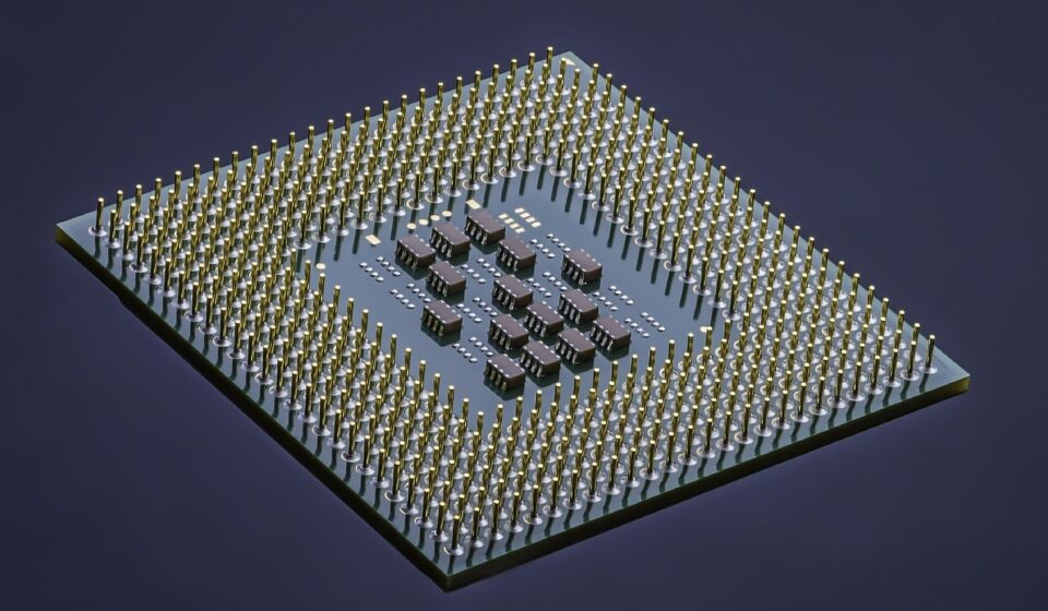
How the semiconductor chip manufacturing process works
The semiconductor chip manufacturing process turns a polished silicon wafer into many finished integrated circuits through repeated cycles of material growth, patterning, removal, measurement, and correction. A chip is not carved in one operation. It is built layer by layer, with transistors formed in the silicon and metal interconnects added above them so that billions of devices can switch and communicate. After wafer fabrication, each die is electrically tested, separated, packaged, and tested again. Intel’s public manufacturing explainers describe modern wafer fabrication as involving thousands of controlled steps over several weeks, while ASML’s lithography materials show why patterning has become one of the most technically demanding parts of advanced chip production.
This guide follows the flow in practical manufacturing terms, from design handoff to final package. For more process-focused industrial articles, visit our manufacturing processes section.
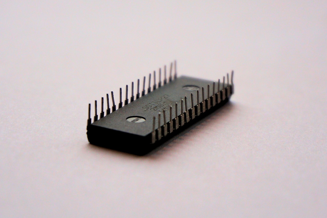
From chip design to a production wafer
Before a wafer enters a fab, the chip design has already gone through architecture, circuit design, physical layout, verification, and manufacturing rule checks. The final layout data is used to create photomasks or reticles, which act as highly precise pattern templates for lithography. The foundry or integrated device manufacturer also relies on a process design kit, often called a PDK, that defines the rules and device models for a specific process node.
Why design rules matter
Design rules are not just documentation. They translate manufacturing limits into layout constraints such as minimum line widths, spacing, via sizes, metal density targets, and reliability margins. A design that violates these rules may be difficult to print accurately or may lose yield after fabrication. That is why manufacturability is checked before tape-out, not only after silicon is returned from the fab.
Wafer preparation
Most logic and memory chips are fabricated on circular silicon wafers, commonly 300 mm in leading high-volume fabs. The wafer must be extremely flat, clean, and uniform because later steps create features measured in nanometers. Preparation may include crystal growth, slicing, polishing, cleaning, and surface conditioning before the wafer is released into the production line. Not every semiconductor product uses the newest wafer size or node. Analog, power, MEMS, radio-frequency, and automotive devices may use mature processes that are more cost-effective for their performance and reliability requirements.
Wafer fabrication builds the circuit layer by layer
Wafer fabrication is the front-end portion of semiconductor manufacturing. Its core purpose is to create active devices, isolate them, and connect them into usable circuits. The exact flow differs by device type, node, and manufacturer, but several unit processes appear repeatedly across most integrated circuit production.
| Process step | Manufacturing role | Why it matters |
|---|---|---|
| Cleaning | Removes particles, films, and residues before sensitive steps | Reduces defect risk and improves surface consistency |
| Oxidation or deposition | Adds insulating, conducting, or semiconducting films | Creates gate dielectrics, spacers, barriers, and interconnect layers |
| Photolithography | Transfers circuit patterns from a mask to photoresist | Defines where material will remain, be removed, or be modified |
| Etching | Removes exposed material using wet chemistry or plasma | Forms trenches, contact holes, fins, and other patterned structures |
| Ion implantation or doping | Introduces controlled impurities into silicon | Adjusts electrical behavior so transistors can switch properly |
| Chemical mechanical planarization | Flattens the wafer surface after layer formation | Keeps later lithography and interconnect steps within focus and thickness limits |
| Metrology and inspection | Measures dimensions, overlay, film thickness, and defects | Feeds data back into process control before yield is lost |
Lithography is often the most visible part of the semiconductor chip manufacturing process because it determines how accurately patterns can be printed. In optical lithography, light passes through or reflects from a patterned mask and projects an image onto a light-sensitive resist. After development, the remaining resist protects selected areas while exposed regions are etched, doped, or otherwise processed. ASML’s lithography documentation describes extreme ultraviolet lithography, or EUV, as using a much shorter wavelength than deep ultraviolet lithography, making it important for selected advanced logic and memory layers. Many layers and many mature-node products, however, still rely on deep ultraviolet or other established techniques because they are less expensive and sufficient for the required geometry.
Deposition and etching work closely with lithography. A film is added, a pattern is printed, unwanted areas are removed, and the wafer is cleaned and measured. This sequence can repeat many times. For an advanced logic chip, the transistor structure, local contacts, and multiple metal layers are produced through a tightly controlled flow. The result is not a single flat circuit, but a three-dimensional stack of devices, dielectrics, vias, and metal lines.
Process control and yield decide whether the flow is manufacturable
A process is not successful simply because it can produce one working die. It must produce enough good die per wafer at a predictable cost. Yield is affected by defect density, design sensitivity, tool variation, overlay error, film uniformity, contamination, and electrical margins. That makes measurement as important as the visible processing steps.
Fabs use in-line metrology to measure critical dimensions, layer thickness, alignment, wafer shape, and surface defects while the wafer is still moving through the line. If a process drifts, engineers can adjust recipes, stop a lot, or route wafers for additional review. Inspection tools do not catch every possible defect, but they support statistical control and help prevent one tool issue from damaging a large amount of work-in-progress inventory.
Cleanroom control is another defining constraint. Particles, ionic contamination, organic residues, and airborne molecular contamination can create shorts, opens, threshold shifts, or reliability problems. Many particles that matter to a modern fab are not visible to the human eye. Production areas therefore use filtered airflow, protective garments, automated wafer handling, sealed carriers, strict chemical control, and disciplined maintenance procedures. The objective is not general cleanliness; it is repeatable contamination control at the scale required by the process.
Wafer probe, dicing, packaging, and final test
After front-end fabrication is complete, the wafer moves into electrical testing and back-end manufacturing. Wafer probe uses automated test equipment and probe cards to contact each die while it is still on the wafer. This step identifies die that meet basic electrical requirements and separates them from defective die before assembly resources are spent on packaging.
The wafer is then diced into individual die. Each good die is attached to a package substrate or leadframe, connected through wire bonding, flip-chip bumps, hybrid bonding, or another interconnect method, and protected with a package structure suited to its thermal, mechanical, and electrical needs. Packaging is not only a protective shell. It provides power delivery, signal routing, heat spreading, and a practical way to mount the chip onto a printed circuit board or into a larger module.
Final test checks the packaged device under defined electrical and sometimes thermal conditions. Some products also undergo burn-in, reliability screening, or application-specific tests, especially when they are used in automotive, aerospace, industrial, medical, or infrastructure systems. A consumer processor, a memory device, a power MOSFET, and a sensor may all follow the broad sequence of fabricate, probe, assemble, and test, but the test program and acceptance criteria can be very different. See also: cnc and robotics.
Advanced packaging is changing where value is created
Historically, many discussions of chip manufacturing focused mainly on the wafer fab. That focus still makes sense because transistor formation and fine interconnects are extremely complex. But advanced packaging has become more strategic as scaling becomes harder and system performance depends more heavily on memory bandwidth, power delivery, and heterogeneous integration.
Chiplet-based designs divide functions across multiple die that can be manufactured on different process nodes and then integrated in one package. This can improve yield economics and let designers combine logic, memory, analog, or I/O functions without forcing every block onto the most expensive leading-edge node. Intel’s public technology materials describe approaches such as embedded bridges and 3D stacking, while TSMC and other major manufacturers discuss wafer-level and 2.5D integration as important for high-performance computing and AI accelerators.
This shift does not eliminate front-end scaling. It changes the optimization problem. Manufacturers now balance transistor density, die size, package substrate capability, interconnect density, thermal limits, power integrity, and supply chain capacity. For buyers of chips or manufacturing equipment, the practical takeaway is that the semiconductor chip manufacturing process increasingly extends beyond the fab into assembly, packaging, and system-level validation.
Capacity, cost, and manufacturing constraints
Modern fabs are capital-intensive because they require lithography scanners, etch tools, deposition chambers, implant systems, cleaners, metrology tools, automated material handling, specialty gases, ultrapure water, and strict environmental controls. A bottleneck in any one area can affect cycle time. Likewise, a new node is not automatically ready for high-volume production when the first devices work; it must reach acceptable yield, reliability, throughput, and cost targets.
SEMI’s 2Q 2026 300mm Fab Outlook projected installed 300 mm fab capacity to rise by about 7% in 2026 and continue growing at a similar approximate rate from 2027 through 2029. That projection is important context because many critical manufacturing steps depend on 300 mm wafer capacity. Capacity alone, however, does not guarantee availability of every chip type. Leading-edge logic, mature automotive devices, power semiconductors, analog ICs, memory, and advanced packaging can face different supply constraints.
Another common misunderstanding is that a smaller process node is always better. For high-performance processors, advanced nodes can improve density and energy efficiency. For power electronics, sensors, display drivers, or mixed-signal products, mature nodes may offer better cost, voltage handling, qualification history, or long-term availability. Manufacturing strategy depends on the product, not only on the smallest published nanometer number.
Frequently asked questions
How long does it take to manufacture a semiconductor chip?
The total time varies by product, node, fab loading, and test requirements. Wafer fabrication alone can take several weeks because the wafer moves through many repeated process and measurement steps. Packaging, final test, qualification, and logistics add more time before a chip reaches a customer.
What is the most important step in semiconductor manufacturing?
No single step is always the most important. Lithography is critical because it defines extremely small patterns, but deposition, etching, cleaning, planarization, metrology, packaging, and test all affect yield and reliability. A weak step anywhere in the flow can reduce the number of usable chips.
Why are cleanrooms required for chip fabrication?
Cleanrooms reduce particle and chemical contamination that can damage tiny circuit features. Semiconductor cleanrooms also control airflow, temperature, humidity, materials, and human interaction with wafers. The goal is stable defect control rather than ordinary workplace cleanliness.
What is the difference between wafer fabrication and packaging?
Wafer fabrication builds the transistors and interconnect layers on the silicon wafer. Packaging happens after the wafer is tested and diced; it connects each die to the outside world, protects it, helps manage heat, and supports final system assembly.
Do all chips use EUV lithography?
No. EUV is used for selected layers in some advanced logic and memory processes, but many semiconductor products are made with deep ultraviolet lithography or other established approaches. The right choice depends on feature size, cost, yield, tool availability, and product requirements.