PCB manufacturing and assembly process, quality controls, and sourcing decisions
What PCB manufacturing and assembly includes
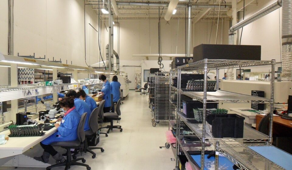
PCB manufacturing and assembly is the connected work of turning circuit design data into a bare printed circuit board, then mounting components so the board can operate inside an electronic product. Manufacturing, often called fabrication, creates the copper pattern, drilled holes, plated vias, solder mask, surface finish, and board outline. Assembly adds solder paste, places components, runs reflow or wave soldering, inspects joints, and performs electrical or functional tests.
Keeping fabrication and assembly in the same workflow helps reduce late design changes, scrap, and reliability risk. Many assembly defects start earlier, either in board fabrication choices or in design-for-manufacturing decisions. A practical review should answer three questions: can the board be made, can the components be assembled repeatably, and can the finished assembly be verified? The answer depends on layout rules, stack-up, materials, component packaging, soldering method, acceptance criteria, and test coverage. For readers comparing this with other production workflows, the manufacturing processes section provides broader context on how industrial process choices affect quality and cost.
From design files to finished boards
Design data review and DFM
The process starts before copper is etched. A fabricator or electronics manufacturing services provider reviews the design package for manufacturability. Typical files include Gerber or ODB++ artwork, drill files, a bill of materials, pick-and-place data, assembly drawings, notes on controlled impedance, stack-up requirements, and test expectations. The DFM review checks whether trace width, spacing, annular rings, solder mask clearances, via structures, panelization, and component footprints are compatible with the intended production process.
This stage matters because a design can be electrically correct and still be difficult to build. Fine-pitch components, microvias, heavy copper, mixed technology, and dense ball grid array packages all narrow the process window. If the design requires controlled impedance, the fabricator also needs dielectric material, copper thickness, target impedance, and tolerance requirements. Missing or inconsistent information often causes more delay than the physical manufacturing time.
Bare PCB fabrication
Fabrication builds the unpopulated board. For a common multilayer rigid PCB, the workflow includes inner-layer imaging, etching, lamination, drilling, desmear, electroless and electrolytic copper plating, outer-layer imaging, solder mask, legend printing, surface finish, routing, and electrical test. The exact sequence varies with board type. A two-layer FR-4 board is simpler than a high-density interconnect design with laser-drilled microvias, sequential lamination, tight impedance, and small annular rings.
Surface finish is one of the choices that connects fabrication with assembly. HASL, ENIG, immersion silver, immersion tin, OSP, and other finishes differ in shelf life, flatness, solderability, cost, and suitability for fine-pitch packages. ENIG is often selected for flatness and wire-bonding compatibility in some designs, while OSP is cost-effective for certain lead-free assembly flows but requires careful handling. No finish is universally superior; the right selection depends on component mix, storage conditions, soldering profile, and end-use reliability needs.
Assembly and soldering
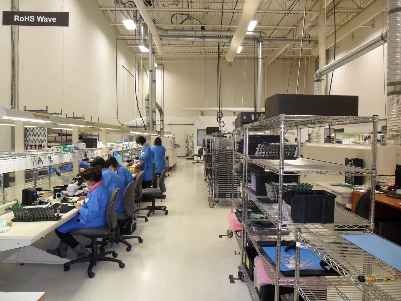
Assembly usually begins with solder paste printing for surface-mount technology. A stencil deposits paste on pads, automated machines place components, and the board passes through a controlled reflow oven. Through-hole parts may be added by selective soldering, wave soldering, or hand soldering depending on volume, geometry, and thermal mass. Mixed-technology boards need special planning because large connectors, heat sinks, press-fit parts, and sensitive packages can conflict with automated soldering steps.
Cleaning is not always a separate step. Some assemblies use no-clean flux systems, while others require cleaning because of coating, high impedance circuits, harsh environments, or customer requirements. The decision should be documented. Residues, ionic contamination, and trapped flux under low-standoff components can become reliability risks. Conformal coating, potting, programming, labeling, and final packaging may follow assembly when required by the product environment.
Materials and design choices that change cost and risk
PCB cost is shaped by more than board size. Layer count, material grade, copper weight, drill density, controlled impedance, via type, minimum line and space, solder mask color, surface finish, panel utilization, and quality requirements all affect price and lead time. Assembly cost is influenced by component count, package mix, placement density, the number of populated sides, stencil requirements, inspection method, programming, test fixtures, and rework risk.
The largest cost increases usually appear when a design crosses a process threshold. Examples include moving from mechanical drilling to laser microvias, from standard FR-4 to low-loss laminates, from simple SMT to fine-pitch BGA assembly, or from visual inspection to X-ray and functional test. Small footprint choices also matter. Selecting an available component package with enough pad spacing may reduce inspection burden and improve first-pass yield.
Panelization is another practical factor. Boards are often produced in panels so they can move through fabrication and assembly equipment efficiently. Poor panel design can waste laminate, create handling problems, or place components too close to breakaway tabs. Designers should confirm rail width, fiducials, tooling holes, edge clearance, V-score or tab routing choices, and depanelization stress limits before release.
Quality controls and standards used in PCB work
Quality control in PCB manufacturing and assembly combines process controls, inspection, electrical testing, and acceptance criteria. Industry organizations such as IPC, UL Standards & Engagement, the European Commission, ECHA, and the U.S. EPA publish standards or regulatory information that manufacturers and buyers use to define requirements. These requirements must be stated in the purchase documents. A supplier cannot reliably meet an unstated class, revision, inspection level, or environmental requirement.
| Document or rule | Where it applies | Why it matters |
|---|---|---|
| IPC-6012F | Rigid printed board performance | IPC announced IPC-6012F in October 2023 for qualification and performance of rigid printed boards, including areas such as microvia reliability and printed board cavities. |
| IPC-A-600M | Bare board acceptability | IPC listed IPC-A-600M as a May 2025 published standard for acceptability of printed boards, supporting visual and workmanship criteria. |
| J-STD-001J | Soldered assembly process requirements | IPC announced the J revision on April 8, 2024, covering soldering materials, process controls, and assembly requirements. |
| IPC-A-610J | Finished electronic assembly acceptability | IPC announced the J revision with J-STD-001J and describes the two as commonly used together for electronic assemblies. |
| UL 796 | Printed wiring board safety evaluation | UL 796 is used for printed wiring board evaluation when board safety recognition is required for the end product. |
| RoHS and REACH | Restricted substances and chemical reporting | EU rules restrict hazardous substances in electrical and electronic equipment, while REACH Candidate List substances can create communication and reporting obligations. |
Inspection methods should match the risk. Bare boards commonly receive automated optical inspection and electrical continuity testing. Finished assemblies may require solder paste inspection, automated optical inspection, X-ray inspection for hidden solder joints, in-circuit test, boundary scan, functional test, or burn-in. A consumer sensor board and an aerospace control board may both use PCBs, but their acceptable risk levels and documentation needs are not the same.
Common failure modes and process limits
Many PCB failures are not caused by one poor operation. They often result from stacked tolerances across design, fabrication, component selection, and assembly. Fabrication-related risks include open circuits, shorts, insufficient copper plating in holes, registration errors, solder mask misalignment, delamination, measling, poor solderability, and impedance deviation. Assembly-related risks include tombstoning, insufficient solder, solder bridges, head-in-pillow defects, voiding, component skew, lifted leads, polarity errors, and heat damage. See also: cnc and robotics.
Thermal management is a recurring limit. Large copper planes, metal-core boards, power components, and mixed thermal masses can make solder profiles difficult to balance. Too little heat may leave weak joints; too much heat may damage components or laminate. Moisture-sensitive components add another control requirement because improper storage or baking can lead to package damage during reflow.
High-density designs bring additional concerns. BGAs and microvias improve routing density, but they reduce the visibility of solder joints and increase dependence on X-ray, process control, and test strategy. When an assembly has limited test access, defects may escape until system-level testing. Early design-for-test review can prevent this by adding test points, boundary-scan access, or fixture-friendly features before the layout is locked.
How to prepare a quote package and evaluate suppliers
A strong quote package reduces assumptions. For fabrication, include board dimensions, layer count, stack-up, material, copper weight, minimum line and space, minimum drill size, surface finish, solder mask and legend requirements, impedance details, acceptance standard and class, panelization needs, and expected quantity. For assembly, include the bill of materials, approved manufacturer part numbers, alternates if allowed, placement data, assembly drawings, polarity markings, solder type, cleaning requirements, inspection requirements, test plan, and packaging instructions.
Buyers should ask suppliers about capability limits, not only price. Useful questions include minimum mechanical and laser drill sizes, standard line and space, controlled impedance tolerance, microvia experience, solder paste inspection availability, X-ray coverage, traceability level, moisture-sensitive device controls, process change notification, and nonconformance reporting. The answers help show whether the supplier is suited for prototypes, volume production, high-reliability assemblies, or only simpler work.
Lead time should be evaluated realistically. Prototype services can produce simple boards quickly, but complex boards need engineering review, material planning, tooling, and sometimes first-article verification. Component procurement may dominate the schedule when parts are constrained, obsolete, or sourced through approved channels only. A low assembly quote can become expensive if the BOM contains unavailable parts, ambiguous alternates, or footprints that do not match the selected packages.
Practical checklist before releasing a PCB build
- Confirm that the schematic, layout, BOM, fabrication drawing, and assembly drawing use the same revision.
- Specify the required IPC class, document revision, surface finish, material, copper weight, and controlled impedance needs.
- Review component footprints against manufacturer land pattern guidance and assembly capability.
- Check polarity, pin 1 marks, fiducials, tooling holes, test points, and panel rails.
- Identify moisture-sensitive, ESD-sensitive, programmed, serialized, or safety-critical components.
- Define inspection and test requirements instead of assuming they are included.
- Confirm regulatory needs such as RoHS, REACH communication, UL recognition, or customer-specific substance restrictions.
- Plan how design changes, concessions, and nonconforming material will be documented.
PCB manufacturing and assembly works best when fabrication, assembly, inspection, and test requirements are designed together. A board that is easy to fabricate but hard to assemble is not optimized. A board that assembles well but cannot be inspected or tested is also risky. The most reliable builds come from early communication between designers, fabricators, assemblers, and quality teams.
Frequently asked questions
What is the difference between PCB manufacturing and PCB assembly?
PCB manufacturing creates the bare board, including copper traces, drilled holes, vias, solder mask, surface finish, and board outline. PCB assembly mounts and solders electronic components onto that board, then inspects and tests the finished assembly.
Which files are needed for PCB manufacturing and assembly?
A typical package includes fabrication files, drill data, stack-up notes, fabrication drawing, BOM, pick-and-place file, assembly drawing, and test requirements. More complex boards may also need impedance tables, approved material lists, programming files, and special inspection criteria.
Why do IPC standards matter in PCB projects?
IPC standards give buyers and suppliers a shared language for board performance, soldering requirements, and acceptability. They do not remove the need for project-specific drawings, but they help define measurable expectations for fabrication and assembly quality.
Is prototype PCB assembly the same as volume production?
No. Prototypes often emphasize speed and design learning, while production emphasizes repeatability, yield, documentation, and process control. A design that works in a small prototype run may still need changes before efficient volume manufacturing.